From sputter cleaning to ion milling: ion beam sputtering
Balancing removal rate and surface damage
The goal of ion beam sputtering is to remove unwanted surface layers as fast as possible without damaging the rest. Damage can be caused for example by overheating and gas incorporation. Contamination of the surface by the ion beam sputtering process itself should also be avoided. This means that ideally the beam size is limited to the sample size to avoid sputtering and redeposition of the sample holder material. Contamination can also be the result of a contaminated ion beam. An important aspect is often the effect of ion beam sputtering on the surface roughness. For most applications it is crucial that the sputter process does not roughen the surface. Important parameters in these processes are the ion energy, current density, and angle of the ion beam with the surface.


Substrate cleaning with ion beams
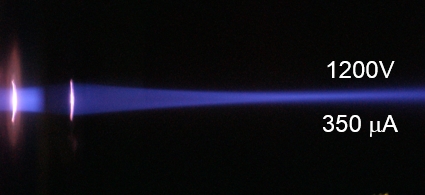
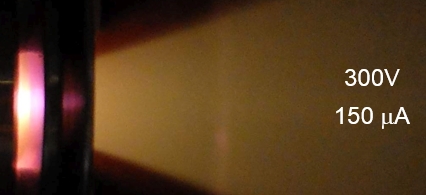
Sputter cleaning is typically done with ion beams with energies of a few hundred volts up to a few kilovolts. All depends on the type of substrate and the amount and type of material or contamination that needs to be removed. For example, adsorbed gases can be desorbed effectively at say 300V, while chemisorbed species require higher energies. The current density of the beam is of the order of 10-100 µA/cm². This range is often a good comprise for substrate cleaning in a reasonable time frame, while limiting the undesirable effects mentioned above.
Sputter cleaning is effective to remove contamination layers or native oxides. It can considerably improve the adhesion if used before thin film deposition.
Ion beam milling
Compared to substrate cleaning, in ion beam milling typically the thickness of material to be removed is larger and the treated sample area smaller, at most a few millimeters. Ion milling with noble gas ions can be seen as physical ion beam etching. Milling with reactive ions is a chemical etching technique. To gain time, ion milling is often done with beams of higher energy and/or with higher current densities compared to sputter cleaning.
Typically a distinction is made between focused ion beam (FIB) milling and broad ion beam (BIB) milling. The majority of FIB milling is done with highly focused and high energy gallium ions (often 30kV). BIB milling is typically done with argon beams up to a few millimeter in diameter, with energies of up to a few kilovolts. FIB milling is very precise, but can induce quite some surface damage (amorphization) and ion implantation. BIB milling has a much lower positional accuracy but is more gentle. Typical current densities in BIB milling are 1-10 mA/cm². It can be complementary to micromachining techniques such as FIB cutting and remove the FIB induced surface damage by ion polishing at low energies.
Nanostructuring with ion beams
Ion irradiation can also be used to adapt the structure of a surface. For example, ion beam sputtering can be used to reveal the internal grain and phase structure of a solid better for analysis purposes. In this case the term ‘ion beam etching’ of the surface also seems appropriate. A relatively large subject is ion beam sputtering to develop a specific surface roughness, e.g. to change the absorption coefficient of solar absorbers, the color of the surface for decorative applications, or the adhesion of biomedical implants.
Ion sputtering & Polygon Physics
Our single cavity ECR ion source TES can be configured to sputter clean samples up to about 4 inch diameter in high vacuum or ultra-high vacuum environment, but also to effectively ion mill with millimeter size beams. The ECR technology delivers stable and reliable beams and does not have the maintenance that technologies based on hot filaments have.
For sputter cleaning and etching of larger surface areas we offer sources based on multiple of our cavities (see HEXAR and our custom beam solutions page for other possibilities).